0 Comments
For decades Moore's law was largely driven by reducing the wavelength and increasing the numerical aperture used for lithography. We've been stuck on 193nm lithography for more than a decade and the next wavelength -- 13.5nm EUV -- has some significant challenges to overcome before it is ready for production. Until then we continue to extend Moore's Law by decomposing complicated photomask patterns into simpler factors. Here's an interesting presentation by AMAT's Chris Bencher that talks about the different flavors of multiple patterning being used today.
http://www.semicontaiwan.org/en/sites/semicontaiwan.org/files/docs/applied_materials_cbencher_litho_forum_2013_for_web_download.pdf
 After completing a trial of the software in May, the Stanford Nanofabrication Facility will permanently install LayoutEditor software on their design servers for the convenience of their users.
If you would like to learn more about LayoutEditor, or are interesting in performing your own evaluation, please see our page How to Use LayoutEditor.  Many thanks to Jason Tresback and Monica Zugravu for the excellent tour of the Harvard Center for Nanoscale Systems.
 Purchase Orders provide a greater level of accounting sophistication and cost allocation. If your procurement system uses purchase orders, simply upload your PO along with your data and layer description file on our HOW TO ORDER A MASK page. Or if you would rather not bother with creating a PO, you can buy directly from our STORE without a PO. Whichever way works best for you.
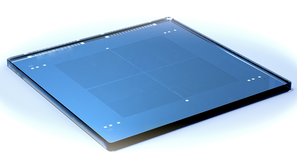
At PhotomaskPORTAL, we provide researchers and small companies with an easy path to low-cost, high-quality photomasks. 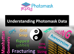 Are you confused about the politically-correct way to specify mask tone? Can't find the tail and not sure which side of the mask is the front and the back? Do you suspect your friends are really saying "Dummy Phil"? Well then ... An updated guide to "Understanding Photomask Data" is available in our store for immediate download at no charge. All comments and upgrades are invited and welcome.
Congratulations to Jay Morreale of p-brane.com for his winning submission in our LayoutEditor contest. Jay put together a two-hour screencast divided into eight individual films that show you how to layout graphene field-effect transistors (GFETs) and associated test structures (Hall, van der Pauw) on a 100mm wafer from start to finish. You can view the videos here.
 There is one day left to submit your entry to our LayoutEditor contest for a chance to win FFFFAB-u-lous prizes (software, photomasks, & training). To enter the contest simply create a video tutorial on any aspect of using LayoutEditor software and upload the video on YouTube. It's that easy.
The tutorial can be on something basic (like how to select objects) or on something complex (like FastCap and FastHenry) -- you decide. You can use an application like QuickTime Player to screencast your video. If you need a temporary license to LayoutEditor to make the video, just ask us for one on our contest page. |