What is a Photomask?
In its simplest form, a photomask is a thin coating of masking material supported by a thicker substrate. The masking material absorbs light to varying degrees and can be patterned with a custom design. The pattern is used to modulate light and transfer the pattern through the process of photolithography which is the fundamental process used to build almost all of today's digital devices.
Photomask Terminology
Here are many of the basic terms you will encounter with photomasks:
Absorber
The masking layer on a photomask is a very thin metallic coating. Popular absorbers in use today are chromium, aluminum, iron oxide, titanium, and silver-halide emulsion. While standard chrome is the work-horse for most photolithography, there are many variations of the oxide thickness on top. You many hear these referred to as low reflectivity chrome (LRC), medium reflectivity chrome (MRC), high reflectivity chrome (HRC), bright chrome, gold chrome, and blue chrome. Aluminum has the highest reflectivity and is useful for laser ablation or gobos. Iron-oxide lets you see through the absorber for alignment purposes while being highly reflective in the UV spectrum. Tantalum boron nitride (TaBN) appears to be the absorber of choice for EUV.
Actinic Wavelength
The discrete wavelength of light the photomask is designed for. Common wavelengths in use today are 193nm (ArF DUV), 248nm (KrF DUV), 365nm (i-line), and 436nm (g-line).
Address Unit
The discrete grid size used to fracture the design data into mask data. See "Fracturing."
Binary Mask
Most photomasks are binary masks, or binary intensity masks, that consist of two tones: clear and opaque. With a binary mask, the mask is either fully absorbing (opaque, dark) where the absorber is present or not absorbing (clear, bright) where the absorber is absent.
Boolean Operations
|
Not every photomask layer has to be drawn. Mask layers can be derived from existing layers with the use of booleans. Boolean operations on polygons lets you derive new polygons from existing polygons. This might be the intersection of two patterns (A AND B), the union of the two patterns (A OR B), the union less the intersection (A XOR B), or one of the two patterns less the intersection (A NOT B; B NOT A) where AND (*), OR (+), NOT (-), and XOR are boolean operations. A common mistake is to use the boolean AND operator when you really want the result of the OR operator. When performing a boolean operation, do it on the lowest level of hierarchy possible.
|
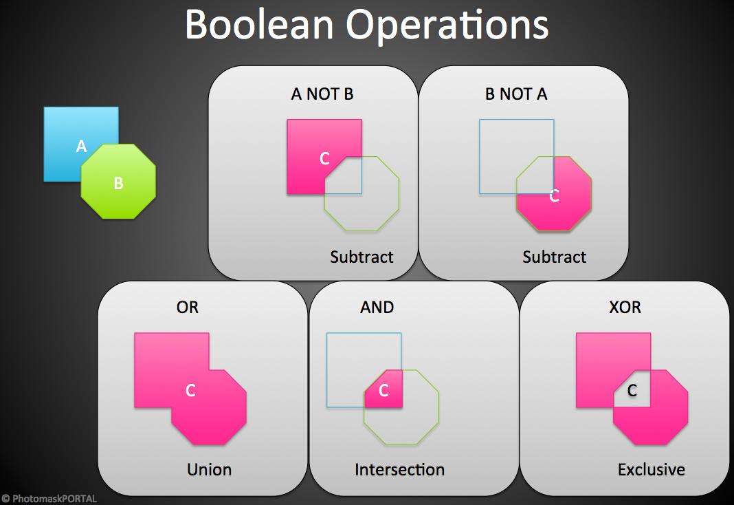
Boolean operations on polygons.
|
Critical Dimension (CD)
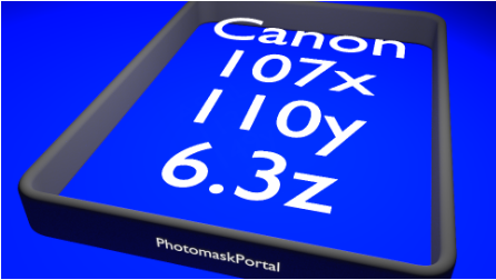
The critical dimension on a photomask is the feature you want produced with the greatest precision. The CD target you specify should be a single type of feature (line/space or contact), a single size, a single loading (isolated or dense), and a single tone. The CD target may be located in one or multiple locations. We will optimize our process to produce the CD with the greatest precision and use it to disposition the reticle against the CD tolerance specification. The CD is often the smallest feature in your layout although it doesn't have to be. More than just for checking dimensions, a CD also gives us a point to verify correct tone and scale, a valuable QC check. We specify at least one CD on every reticle we build and the deviation from this target will be shown on the label attached to the mask compact..
CD Tolerance
The CD tolerance is the most common specification for a photomask and verifies a degree of dimensional accuracy is met. It is the maximum allowable deviation from the nominal CD target. This specification can be absolute or based on the average (mean to target).
CD Uniformity
The CD uniformity is the range of CD readings, the difference between the maximum reading and minimum reading, expressed absolute or 3-sigma.
Centrality
Centrality measures how well the pattern is centered on the substrate. Centrality doesn't matter for many 1X masks where alignment is done manually but will be specified at 0.5mm or less for stepper reticles.
Chrome
Chrome is well-established as the standard absorber for photomasks due to it's opacity, durability, and adhesion properties. What we refer to as "chrome" is actually a stack of pure chromium (Cr, 80-100nm thick) topped with a layer of chromium oxide (Cr203, 10-30nm thick). This very thin stack (~100nm) is easy to process, provides an optical density of 3.0, and the chromium oxide, serving as an anti-reflective coating, minimizes reflection that would double-expose the resist. Chrome adheres well to the glass substrates and the chromium oxide adheres well to photoresist.
Chrome-Up / Chrome-Down
Masks are typically viewed, used, and handled in a horizontal position where one side is facing up and the other is facing down. If the chrome (or generically the absorber) is on top of the glass (or facing you), we call this CHROME-UP. Alternatively, if the chrome is on the bottom of the glass (or facing away from you), we call this CHROME-DOWN. Closely tied to this terminology is mask "PARITY".
Closure Check
A closure check is a type of quality control performed during photomask manufacturing. A small pattern will be written on the side of the photomask at the very beginning of the exposure and then a complementary mark will be written right beside it at the very end of the exposure. If the two patterns align with each other, this insures there was no drift during the exposure process.
Compact
The plastic box or case the photomask ships in is commonly called a compact.
Data
Your "data" can be a reference to your mask design file (the database, as in "Please send your data") or to the enclosed polygons in your design (the digitized data, as in "What tone is your data?"). Digitized data may not be the same as your features depending on how your data is drawn and if it has been reversed. Read more about mask design concepts.
Database
The database is another name for your mask design file.
Dataprep
Mask DataPrep (MDP) is the process of preparing your design data for manufacturing. Normally a mask designer will output the design in an interchange format such as OASIS or GDS-II that is not specific to the mask manufacturing equipment. MDP will convert the data from the interchange format to the specific format needed by the pattern generators, apply sizing needed for the etch process, perform any additional transformations (scale, rotation, offset, booleans operations), and create jobdecks and metrology files.
Defects
A defect is considered anything that will print on the wafer and negatively impact the device. These can be hard defects involving the patterned absorber (a chrome bridge between two lines) or soft defects (fall-on particles). For more advanced masks, we use AIMS software to determine if a defect will print in a given fab process.
Die
A die is the fundamental design element, or device, on a photomask. Often a single die will be arrayed on a reticle inside of a frame.
Digitized Data
A mask design consists of two distinct areas: the area inside polygons and the area outside polygons. Digitized data is the area INSIDE polygons. If you tell us you want the Digitized Data to be clear, will will make the area inside the polygons clear on the mask. See "Data."
Emulsion
Silver-halide emulsion is another type of absorber. Emulsion can achieve the necessary opacity but is easily damaged and greatly affected by humidity and temperature. While you seldom see emulsion used anymore on glass, it is still commonly used on film masks.
Etch
After your pattern is produced in the photoresist, it must be transferred to the absorber by either wet- or dry-etch. Wet-etching with acid is an isotropic process whereas dry-etching with plasma is anisotropic. Additional bias or sizing is applied to your data to account for the type of etch process being used. In short, the clear features in your design data will be written slightly smaller on the mask so they can grow laterally to the target size during the etch process.
Exclusion Zone
Depending on the pattern generator being used, you may not be able to expose a pattern all the way to the edge of the photomask. Even if you can, you shouldn't write any critical patterns, such as your CD, as the quality of the photoresist and absorber degrade near the edge of the photomask, especially in the corners. An exclusion zone tells you how far away to stay from the edge of the photomask. These zones normally vary between 3 to 10 millimeters. Patterns can often be written all the way to the edge of the mask but the quality may be a little suspect right near the edge.
Feature
There are two basic types of features on a photomask: lines (and complementary spaces) and contacts. For example, metal layers often consist of lines and spaces whereas via layers consist of contacts. The distinction is made because lines and contacts print differently on a photomask, especially as the feature size gets small. The minimum feature size on a mask is the smallest feature in your design data. The minimum feature size on a mask is not the same as the critical dimension or the resolution limit or the minimum features size that the overall lithographic process is capable of resolving.
Fiducial Package
The fiducial package refers to the collection of patterns that are outside of the active area on a mask or reticle and often consists of alignment marks, mask processing marks, titles, barcodes, and logos.
Film Masks
Also known as transparency masks, film masks consist of an absorber of emulsion on a substrate of polyester film. They can be exposed with a photoplotter with resolutions that normally range between 4k to 40k dpi. These masks can provide quick and cheap prototyping when features sizes are at least 10um and longevity and dimensional stability is not a concern. In use, film masks will normally be taped to a bare substrate and used in a 1X aligner in lieu of a chrome mask. Film masks have an opaque layer of silver-halide emulsion coating on one side of a clear polyester film. Mylar is perhaps the most well-known brand of this type of polyester material (specifically biaxially-oriented polyethylene terephthalate) registered by E.I. DuPont de Nemours in 1952 and currently owned by DuPont Teijin Films US.
Flatness
The flatness of a mask is measured as the total indicated range (or peak-to-valley) over a given area. Flatness is often reported as either "C" (over a circular area) or "T" (over a rectangular area). The thicker the substrate, the less sagging will occur when the mask is mounted horizontally for exposure.
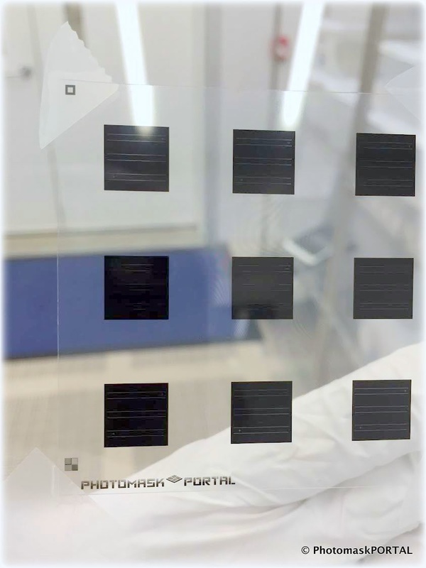
FPD Masks
|
The same photolithography process used to build semiconductor devices on a wafer is used to to fabricate flat panel displays. But the masks are MUCH larger. Generation 8 (G8) FPD masks are made with a chrome absorber on a quartz substrate that measures 1.22m x 1.40m and 13mm thick. Generation 10 FPD masks will average 1.7m per side.
|

Photo courtesy of Photronics PKLT.
|
Fracturing
|
The elements that modern CAD and EDA software are capable of generating is often much more sophisticated than the primitive elements used by the pattern generator to expose the mask. Fracturing converts the polygons in the layout interchange data into the specific format accepted by the pattern generator tool, namely various types of trapezoids. During fracturing, other operations including scaling, sizing, mirroring, rotation, and booleans may also be performed. Reducing the number of vertices you use when approximating a circle or curve in your mask design will reduce the number of trapezoids required in the fractured mask data (the "trap count") and make your mask write faster. Shown below is a circle that was approximated by a 16-sided regular polygon in the mask design file and by seven trapezoids in the fractured mask data.
|
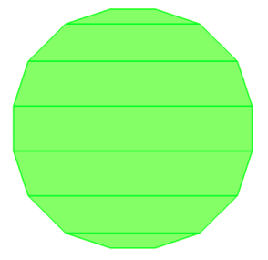
Transformation of a Circle (design concept) to a hexadecagon (gds-II) to seven trapezoids (mask data).
|
Frame
A frame, also called the scribe, kerf, or street, is a orthogonal pattern designed to contain the primary die patterns. The frame will contain various test and metrology marks used for process control during wafer fabrication and is typically built by the fab once they know the size of the primary patterns. After wafer fabrication, the frame area will be used to dice the wafer into individual chips.
GDS-II
Introduced in the mid-1970s by the Calma Company, this data format, pronounced "G-D-S-2", is the industry standard format for physical layout interchange. GDS-II is the most widely used format for mask design data.
Inspection
There are various types of defect inspection. Pattern inspections including die-to-die inspection (looking for differences between actual die on the photomask) and die-to-database inspection (looking for differences between actual die and the design data) are usually done before a pellicle is applied. STARlight and QC Optics inspections, based on scattering of incident light, are usually done after a pellicle is applied. Visual or manual inspections using bright lights or microscopes is done throughout the process.
Iron Oxide
Iron oxide is an absorber that is transmissive in the optical spectrum while opaque in the ultraviolet. This lets an operator visually see through the absorber for alignment purposes while simulataneously using the mask to attenuate UV wavelengths.
Jobdeck
A jobdeck is a control file that tells the pattern generator where and how to place patterns and titles.
Layers and Data-types
Originally photomasks served as simple stencils of a given process layer in the semiconductor manufacturing process. There was a one-to-one association between the layers in the fab process and the layers in the mask design file. Modern practice is there are many more layers of abstraction in the design file than there are layers in the fab process or layers in a mask set. There are sometimes over a thousand layers to choose from in the design file and each layer can be further divided into over a thousand datatypes. The Mask Order Form you provide with your design data will tell us how to map the layers and datatypes in your design file to the masks being built.
Layout
This refers to the physical layout of an abstract symbolic design. Resistors and capacitors on an electrical schematic get transformed into a physical representation during layout. After the layout has been rigorously checked against design rules, the layout is taped-out in gds-II or OASIS format for mask fabrication.
Lithography
See "Photolithography."
Manhattan Geometry
|
Much of the equipment used to manufacture photomasks, such as pattern generators and inspection and metrology tools, was designed for Manhattan Geometry, or "axis-aligned orthogonal" data that is either parallel or perpendicular to the two major axes. Adding in 45-degree angles, or "axis-aligned octangular" data is okay. Circular data that is curvy -- such as a waveguide design -- can dramatically increase write time and file size as the number of trapezoids needed to approximate these curves greatly increases.
|
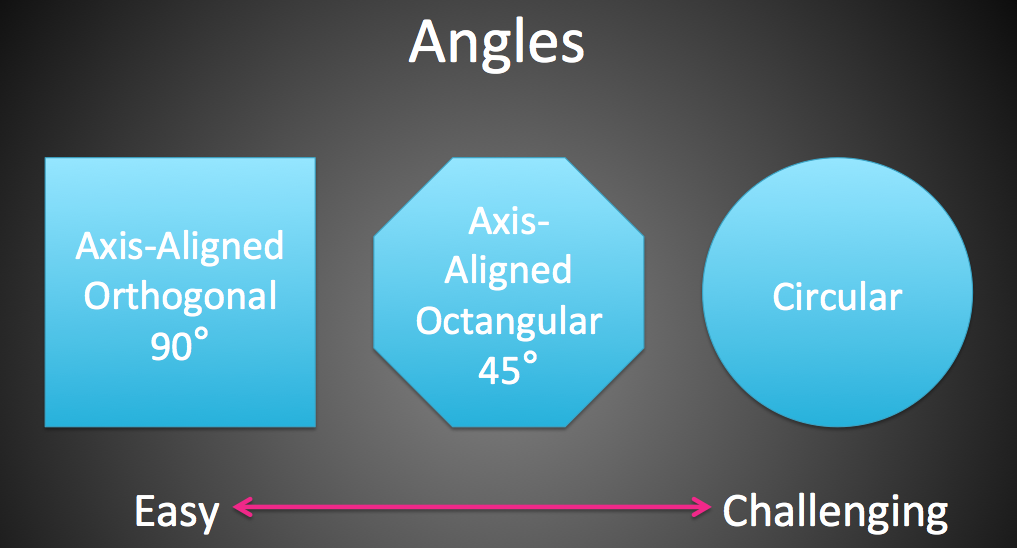
Degrees of angularity on a photomask.
|
Manufacturing Grid
Pattern generators can be vector-scan or raster-scan. While a vector-scan tool can move along any vector, a raster-scan tool will impose a uniform grid (a raster) on the pattern data. Regardless of what grid you used to design the pattern, it will be forced to the manufacturing grid -- or address unit -- of the pattern generator. The manufacturing grid for most pattern generators ranges from 1 to 250nm and is significantly smaller than the minimum resolution of the photomask process. When designing a mask, your design grid should be an even multiple of the manufacturing grid to avoid grid snapping. For example, if you intend to print a film mask on a photoplotter with a 4k dpi manufacturing grid, your design grid should be a multiple of 6.35um (25400 / 4000). A 50um feature would snap by 0.8um whereas a 50.8um feature would not.
Mask Order Form (MOF)
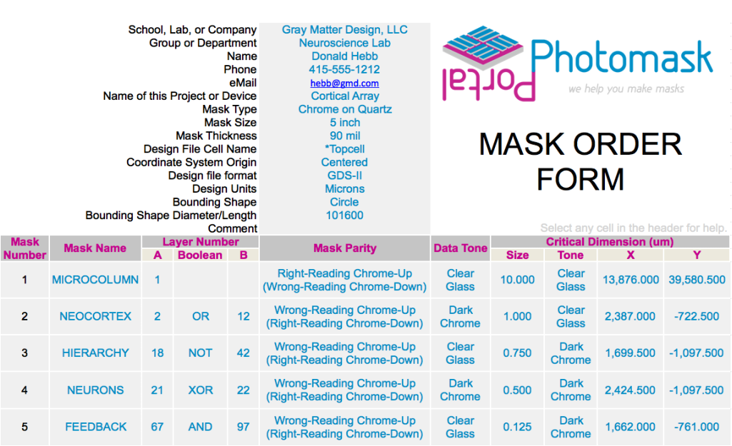
The mask order form contains the essential information needed to build a photomask that is not contained in the mask design file. For each mask, at a minimum we need to be told the mask name, the gds layer number, the tone (polarity) and mirroring (parity) specifications, the size, feature type, location, and tone of the critical dimension (CD). More sophisticated mask orders follow the P10 specification of the SEMI organization.
Masters and Sub-Masters
A direct-write 1X photomask that is used to expose a wafer is referred to as a "master". This is distinguished from a direct-write 1X photomask called a "sub-master" that is used to print copies of itself (copy plates). The key difference between a master and a sub-master is opposite parity. While masters are typically wrong-reading, sub-masters will be right-reading.
MEBES
MEBES, pronounced "meebus" (not "meebz"), was the name of the industry's first eBeam tool in the late 1970s. The Manufacturing Electron Beam Exposure System was invented at Bell Labs and commercialized by ETEC. The data format used by this tool (MEBES data) became an industry standard which is still widely used.
OASIS
Introduced in 2002 by the SEMI organization, the Open Artwork System Interchange Standard (OASIS) is the data interchange format intended to replace GDS-II. While it offers numerous improvements over GDS-II, most notably OASIS reduces file size by some 90%. Today it is the prominent format used by large companies while GDS-II remains entrenched with more mainstream users.
Optical Density
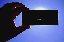
If you hold a chrome mask up to a light, you can vaguely see the light shining through the chrome, much like the light leaking through a solar eclipse filter or welding goggles.
The purpose of the metallic coating on a photomask, such as chrome, is to attenuate the intensity of light enough that photoresist on the other side will not be activated. We want the coating to be thick enough to attenuate most of the light, but we also want it as thin as possible to get the best dimensional control on the mask since the thinner the chrome, the less etching is required. So decades ago, when the industry standardized on chrome as the absorber of choice, it was determined that an optical density of 3.0 was sufficiently opaque at common exposure wavelengths in the UV spectrum.
Technically, optical density is the amount of attenuation -- or gradual intensity loss -- that occurs when light passes through an optical component. Mathematically, optical density is a logarithmic scale of how much light is transmitted through the absorber material: OD = Log (Power transmission factor).
For example, an optical density of 3 attenuates the light power by a factor of 10^3 (1,000). An optical density of 4 attenuates the light power by a factor of 10^4 (10,000). This optical attenuation may result from not only absorption of light but also from scattering of light. Absorbance, a closely related term, considers only absorption within the optical component but not scattering.
Transmitted Light Optical Density
100.00% = 1.0000 = 1x10^0 0
10.00% = 0.1000 = 1x10^-1 1
1.00% = 0.0100 = 1x10^-2 2
0.10% = 0.0010 = 1x10^-3 3
0.01% = 0.0001 = 1x10^-4 4
100.00% = 1.0000 = 1x10^0 0
10.00% = 0.1000 = 1x10^-1 1
1.00% = 0.0100 = 1x10^-2 2
0.10% = 0.0010 = 1x10^-3 3
0.01% = 0.0001 = 1x10^-4 4
A photomask will typically have a base layer of chrome between 80 to 100nm thick (not including the chrome oxide on top of it) to achieve an optical density of 3.0 in the UV spectrum. For exposure wavelengths in the deep UV, such as 193nm, the balance is shifting towards thinner chrome (and lower optical density) in pursuit of better control of smaller features.
Optical Pattern Generators
Before pattern generators used LASERs and eBeams to expose the pattern, there were optical pattern generators. These original PG tools used optical lithography to write a mask. Similar to how a stepper uses a photomask to expose a wafer, optical pattern generators would move and rotate a physical aperture between a light source and a photomask. Over the course of several days and tens of thousands of shots, an entire photomask would be exposed.
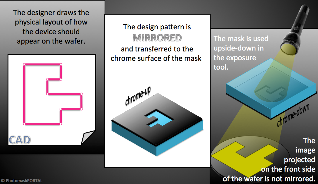
Parity
|
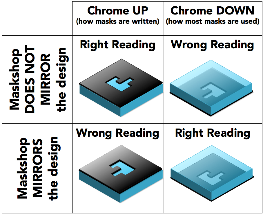
Masks are always written chrome-up but are commonly used chrome-down. If the pattern you design for a photomask is not "mirror symmetric", it will appear as a normal image from one side of the mask and a mirror-image from the opposite side.
|
|
|
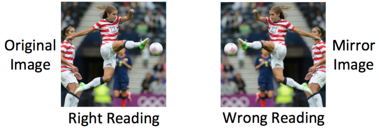
To clarify, we borrow terminology from photography called Right-Reading and Wrong-Reading. In photography, the original image is defined as Right-Reading and the mirror of the original image is called Wrong-Reading.
|
|
In photolithography, we define the original design pattern you supply (whatever that may be) as Right-Reading and the mirror image of the design pattern as Wrong-Reading. Typically the original design will have normal (unmirrored a.k.a. right-reading) text and the mirror of your design will have mirrored or wrong-reading text.
|
To specify mask parity you must state both the image parity (right-reading or wrong-reading) and the frame of reference (chrome-up or chrome-down).
|
|
Note that there are only two possible mask combinations since Right-Reading Chrome-Up is the same physical mask as Wrong-Reading Chrome-Down and Wrong-Reading Chrome-Up is the same physical mask as Right-Reading Chrome-Down.
The important thing to note is that if you specify Wrong-Reading Chrome-Up (or Right-Reading Chrome-Down) on the mask order form, we will mirror the design you supply before writing it on the mask.
Pattern Generator (Mask Writer)
The pattern generator, as the name implies, is the tool that exposes a latent image of the mask design data in the photoresist of a photomask. The first PG tools (Electromask, David Mann) used optical lithography, which were replaced by eBeam tools such as the MEBES by ETEC, and eventually LASER tools, such as the CORE and ALTA platforms built by ATEQ (subsequently ETEC, subsequently AMAT). There are numerous current suppliers including Micronic, Heidelberg, Leica, Jeol, Hitachi, and Toshiba.
Pellicle
The pellicle is an ingenious device that greatly extends the lives of photomasks used in projection printing by keeping air-borne particles far enough away from the mask plane not to print. Pellicles are very thin membranes of a highly transmissive material that are supported by an aluminum frame. On mainstream steppers from ASML, Canon, and Nikon the membrane is specified to be a distance of 200 to 250mil away from the absorber. 5" masks that are 90mil thick require a pellicle on both sides. 6" masks require only a single pellicle on the chrome-side since the 250mil substrate provides adequate separation. ASML is developing a pellicle for use with EUV which has to withstand the barrage of high-energy photons at 13.5nm not once but twice due to the reflective optics of EUV.
Photolithography
Photolithography is essentially a patterning technology using light as the transfer medium. This is the fundamental process used to mass-produce the integrated circuits and electrical components used inside almost all of today's digital devices. In basic terms, the process of photolithography involves:
- A silicon wafer or a thin film of chrome on a photomask(i.e. the substrate) is covered with a layer of photo-sensitive polymer (a photoresist).
- We expose the polymer with a pattern of light. Depending on the type of polymer used, it either softens or hardens where it is exposed to light.
- The soft polymer is washed away leaving a pattern of hard polymer on top of the substrate. We use this hard polymer as a template to etch the substrate.
- We etch the exposed substrate (where the polymer was removed) with an acid (wet etch) or a plasma (dry etch).
- The hard polymer is then removed leaving the substrate (silicon wafer or chrome) etched with the same pattern that was exposed with light.
Photoresist
A chemical solution that is affected by light. A positive resist will become soluble where exposed to light; a negative resist will harden or crosslink with exposure to light. After the resist has been exposed and developed, it will serve as an etch template to transfer the pattern to the absorber, after which the remaining resist will be stripped away.
Polarity
See "Tone."
Polygon
A polygon is a 2D closed chain of line segments connected by vertices. The initial point of a polygon is the same as the final point, forming a vertex that closes the polygon. In AutoCAD this is a polyline, not individual line segments. The interior of a polygon is called the body. The tone of a mask is the tone you designate for the body of the polygons. See "Data," "Tone," and "How to Use LayoutEditor."
Quartz
What we refer to generically as "quartz" is technically synthetic fused silica, pure silicon dioxide in amorphous form. It contains no impurities affording superior optical and thermal properties. Although costlier to manufacture than soda-lime, quartz is stronger, withstands higher temperature, has a much lower coefficient of thermal expansion, and wider range of transparency in the deep UV and near IR, and a flatter surface, keeping your pattern in plane.
Reduction
Most photomasks come in one of three scales: 1X, 4X, and 5X. This corresponds to the reduction optics between the mask and the wafer. 1X is simply a 1:1 transfer and there is no reduction while 4X reduces the mask dimensions by a factor of 4 and 5X reduces the mask dimensions by a factor of 5. 1X is used for contact and proximity printing while 4X and 5X are used for projection printing. 5X is typically found on older steppers while 4X is the reduction of choice on newer scanner systems including EUV.
Registration
In addition to dimensional accuracy (the CD), you also want good positional accuracy. We call this registration-to-grid and it represents the lateral displacement of a given point to where it should be relative to an ideal grid. Generally the positional accuracy is a function of the pattern generator used to expose the mask but it can also be affected by the flatness or skew of the mask surface.
Reticle
A "reticle" is a type of photomask that is designed to be stepped in an array around the wafer. These are typically used in a 4X or 5X reduction stepper or scanner. A photomask used for contact printing where the mask is not stepped around the wafer is simple called a "mask."
Right-Reading
This term refers to the original pattern you supplied. By definition the pattern you supply in your design file is "Right Reading". If a mirror operation is subsequently performed on the original pattern, it will become "Wrong Reading." See "Parity."
Sizing
Sizing is a bias applied to your digitized data to account for lateral edge growth during etching. The type of sizing your apply depends on the type of photoresist (positive or negative) and the type of etch (wet or dry).
Sizing is typically applied both in the mask process (by the maskshop) and in the wafer process (by the mask designer). You'll want to be clear which process you are referring to but the concepts apply equally well to both.
Sizing is typically specified at drawn dimensions (1X) before reticle scaling is applied. Sizing is typically applied "per side". Sizing per side means the distance each edge of a polygon moves towards the interior or exterior of the polygon. For example, a square that is 1.25um per side that is sized -0.125um per side will shrink the square to 1.00um per side, a total shink of -0.25um in both X and Y dimensions. You'll want to be clear if you are referring to the total change in the feature size or the sizing per side.
 Wet etch undercut with a 1.3 lateral etch rate.
For an isotropic wet-etch process, where you etch laterally at close to the same rate you etch into the material, you will want to decrease the size of the clear area on the mask (or the exposed area on the wafer for a positive resist) so you can grow it back to the target size during the etch process. This means you will want to shrink your digitized data if it is clear and grow (or bloat) your digitized data if it is dark.
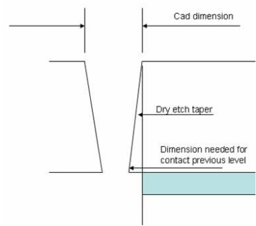 Dry Etch Taper.
For anisotropic dry-etch processes where there is much less lateral edge growth, the resulting steep tapered walls will have slightly smaller dimensions at the bottom than at the top. In this case you may want to grow the clear area with sizing.
See "Etch" for more details.
See "Etch" for more details.
Slivers
Often a photomask manufacturing process will be characterized by the minimum size of feature that can be resolved. Features in a photomask pattern that are smaller than this limit are called sub-resolution features or slivers and may resolve partially or may not resolve at all. Slivers are problematic for die-to-database inspections.
Soda-lime
Soda-lime masks are an improvement over film masks but not as good as quartz masks. In addition to silicon dioxide, soda-lime glass (aka "window glass") has numerous additives such as soda (sodium carbonate) and lime (calcium oxide) designed to lower the melt temperature. Soda-lime is more affected by temperature variation resulting in greater overlay error if you are stacking multiple layers. The flatness of soda-lime masks typically ranges from 5 to 15 microns and the additives present in soda-lime limit transmission in the UV spectrum compared to quartz.
Substrate
The substrate supports the mask absorber. It needs to be transmissive at the actinic wavelength, have low reflectance, and be polished to a flat surface. Most mainstream photomask substrates are made from amorphous fused silica (aka quartz). For low-budget prototyping, soda-lime is also an option although the price savings versus quartz is not as great as it once was. Substrates for the reflective optics of EUV are neither quartz nor soda-lime and simply need to be flat with the lowest possible thermal expansion.
Tape-out
This term goes back to the 1960's and 70's when designers would save their design to state-of-the-art magnetic tape and send these reels of tape to the local maskshop. Today "taping-out your design" is simply an expression for sending your mask design for fabrication, by whatever means, but almost certainly NOT by magnetic tape.
Tone
A binary mask will have two tones: 1) Opaque (dark, absorbs light) and 2) Clear (bright, transmits or reflects light). Unfortunately nowhere in the mask design file (the gds-II data) is there a field to define the tone. The colors displayed by the EDA software are simply there for our convenience and have nothing to do with mask tone. You can tell us the tone of your data via documentation such as the Mask Order Form. The simplest way to do this is to specify the tone of the polygon bodies in your data and to specify the tone at a point on the mask (the CD).
Topcell
Data formats such as gds-II and OASIS promote data hierarchy. If an element in the design repeats, you will only draw it once and then place instances of this element throughout your design. You draw these elements in cells and give the cells unique names. Small cells are combined to make medium cells; medium cells are used to draw large cells. Eventually all of these cells come together in a single cell at the top of the hierarchy. This is the (or a) "top cell". When we ask for the topcell, we are asking for the cell (and all its underlying hierarchy) you want us to use to build the masks. The cell you give us to build your masks (our topcell) doesn't have to be the top of the hierarchy in the file (your topcell).
Wrong-Reading
This term refers to the mirror-image of the original data you supplied. See "Parity."
More Advanced Terms
Double-Patterning
Double-patterning replaces a very challenging lithography step (with one expensive mask) with two simpler lithography steps (and two less expensive masks). You are trading off the additional cost and time required for a second patterning step for the simplification of the mask design. This concept can be extended to more than two masks.
Dummy Fill
|
Dummy fill is uniformly-spaced square-patterns added to a design to aid processing. Dummy fill provides more uniform pattern loading during plasma etching and produces a more planar wafer surface for CMP polishing. Dummy fill serves no electrical purpose and should have relaxed specifications.
|
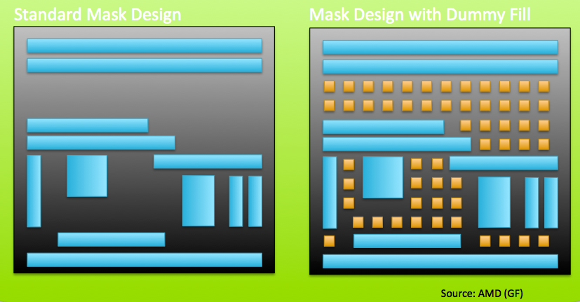
Dummy Fill applied to photomasks.
|
Extreme UltraViolet Lithography (EUV)
|
Extreme ultraviolet lithography uses a wavelength of 13.5nm. Since there are no transparent materials at this wavelength, the optics must change from refractive to reflective. Instead of having a series of refractive lenses, the exposure tool has a series of reflective mirrors. The photomask itself is one of these mirrors but has a patterned absorber on its surface. Instead of attenuating the intensity of light as it passes through the photomask like a chrome mask does, an EUV mask reflects light where the absorber is absent and absorbs light where the absorber is present, projecting a pattern of light down the series of mirrors until it eventually exposes a resist-coated wafer. In the following image of the inside of an EUV scanner built by ASML, the path of light from the EUV source to the wafer is shown traced with yellow rays.
|
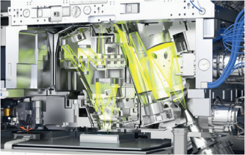
ASML TWINSCAN NXE:3300B EUV Lithography Scanner
|
Grayscale Lithography
Grayscale is the application of features on the mask that are large enough to resolve on the mask but too small to resolve on the wafer. Even through these features are too small to resolve independently, their aggregate effect is felt and can be used to sculpt the photoresist in the third dimension.
Immersion Lithography
Immersion lithography is a resolution enhancement technique that, along with double patterning, has sustained Moore's law for the last several years while EUV is fully developed. It works by replacing the air gap between the projection lens and the wafer with water.
The resolution limit may be expressed as
R = k x λ / NA
where
NA = n x sinθ
where
R = k x λ / NA
where
- K is a process factor,
- λ the wavelength of light, and
- NA is the numerical aperture of the lens system
NA = n x sinθ
where
- n is the refractive index of the medium between the projection lens and the wafer and
- θ is the angle of incidence of light on the wafer.
Optical Proximity Correction (OPC)
|
As features on the mask become smaller than the actinic wavelength, non-linear diffraction effects start to dominate causing increased corner rounding and line-end shortening. These effects can be offset with various levels of OPC that range from biasing the data to adding serifs and sub-resolution assist features. The OPC can be driven by simple rules (rules-based) or a model of the lithographic process (model-based).
|
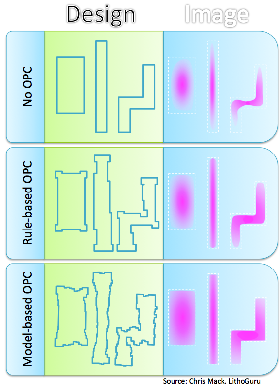
Types of photomask OPC.
|
Phase-Shift Mask (PSM)
Binary masks modulate the intensity of the light without changing its phase. Phase-shift masks, on the other hand, modulate the phase without changing the intensity (hard shifters) or do a weak modulation of the intensity while doing a full modulation of the phase (soft shifters). Hard-shifters (alternating aperture PSM) are made by etching into the quartz substrate the equivalent of half of the optical path and soft-shifters (attenuated embedded PSM) are made by using molybdenum silicide (MoSi) sufficient to shift the phase of the light by 180 degrees while still transmitting about 6% of the intensity. For further reading I refer you to the excellent instruction of Chris Mack at www.lithoguru.com.
Resolution Enhancement Techniques (RET)
Resolution Enhancement Technique refers to any technique used to improve the resolution of a photolithography system such as wavelength reduction, off-axis illumination, double-patterning, and immersion lithography. Resolution enhancement techniques that are specific to photomasks include OPC and phase shifting.
Thin Chrome
As feature sizes written in chrome decrease, the aspect ratio of chrome height to feature width become problematic which creates the need for thinner chrome.